In-depth Analysis of the Welding Process for PUSR IoT Router: Solving the Cold Solder Joint Problem and Establishing the Foundation for Industrial Communication Reliability
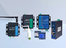
In the era of the Industrial Internet of Things (IIoT), IoT routers serve as the core devices connecting the physical and digital worlds, with their reliability directly determining the continuity of production systems and the stability of data transmission. According to statistics, over 35% of communication interruptions in industrial scenarios stem from electronic component soldering defects, with cold solder joints being the most common type of poor soldering. Due to their concealed nature and random failure manifestations, cold solder joints have become an "invisible killer" plaguing industrial electronics manufacturing. This article provides an in-depth analysis of how PUSR IoT router solve the cold solder joint problem through precision welding processes from three dimensions: welding process principles, the PUSR process control system, and cold solder joint prevention mechanisms, offering industrial customers highly reliable communication solutions.
A cold solder joint refers to a phenomenon where a good intermetallic compound (IMC) is not formed between the solder and the component lead or PCB pad at the solder joint, resulting in intermittent electrical connections. Its hazards are mainly manifested in three aspects:
Concealment: Cold solder joints appear identical to normal solder joints externally and are difficult to detect through traditional visual inspection. Problems can only be exposed through X-ray inspection or functional testing.
Randomness: Cold solder joint failures usually manifest after the equipment has been in operation for some time, influenced by factors such as temperature changes and mechanical vibrations, increasing the difficulty of fault localization.
Destructiveness: The contact resistance of cold solder joints can cause local heating, accelerating solder joint oxidation and ultimately leading to solder joint detachment or circuit board burnout, resulting in significant economic losses.
According to industry data, nearly 50% of electronic device failures are caused by poor soldering, with cold solder joints accounting for over 60%. In industrial scenarios, cold solder joints can lead to production line shutdowns, equipment malfunctions, data loss, and other serious consequences, becoming a key bottleneck restricting the reliability of the Industrial Internet of Things.
The formation of cold solder joints is the result of multiple factors working together, mainly including:
Component factors: Lead oxidation, insufficient plating thickness, and lead deformation can lead to poor contact between the pad and the lead.
Substrate factors: PCB pad oxidation, contamination, and deformation can affect solder wettability.
Process factors: Insufficient soldering temperature, too short a time, and poor flux activity can result in incomplete melting of the solder.
Environmental factors: High humidity and dust pollution in the workshop can accelerate solder joint oxidation.
The difficulties in preventing cold solder joints lie in:
Narrow process window: The soldering temperature must be precisely controlled at 20-30°C above the melting point of the solder. Excessive temperatures can damage components, while insufficient temperatures can lead to cold solder joints.
Multiple variables: Component materials, PCB thickness, and flux type all affect the soldering results, requiring customized process parameters for different products.
Detection difficulties: Traditional AOI inspection can only identify abnormal solder joint shapes and cannot detect the quality of the IMC layer, necessitating the use of X-ray, pull testing, and other methods.
PUSR IoT routers adopt a composite welding process combining surface mount technology (SMT) and laser soldering technology, controlling the cold solder joint rate to below 0.01% through full-process control encompassing "material control - process design - process control - inspection verification."
The SMT process achieves high-density integration and automated production by directly mounting components on the PCB surface. The core control points of the PUSR SMT process include:
Solder Paste Printing: Laser-cut stencils are used to control the solder paste thickness within the range of 0.12-0.15 mm, ensuring uniform coverage of the pads. SPI (solder paste inspection) equipment is used to monitor parameters such as solder paste volume, area, and height in real-time, controlling the printing defect rate to below 0.01%.
Component Mounting: High-speed placement machines (such as Siemens HS60) are used to achieve placement accuracy at the 0.1 mm level through a visual positioning system, supporting the placement of small components such as 0402 and 0201. Anti-static measures and temperature and humidity control (25°C ± 3°C, RH 45% ± 10%) are introduced during the placement process to avoid component performance drift.
Reflow Soldering: A ten-zone reflow oven is used to precisely control the temperature curve (preheat zone 120-150°C, soak zone 150-180°C, reflow zone 235-245°C, cooling zone ≤ 5°C/s) to ensure the formation of a good IMC layer at the solder joints. For large-sized components (such as power modules), separate temperature parameters are set to avoid thermal stress damage.
AOI Inspection: Optical inspection technology is used to conduct a full inspection of solder joint morphology, component polarity, and placement position, combined with X-ray inspection for perspective analysis of hidden solder joints such as BGAs and QFNs, achieving 100% quality traceability.
To address the limitations of traditional soldering processes in scenarios such as micro pads and flexible substrates, PUSR introduces laser soldering technology, solving the cold solder joint problem through its core advantages of "non-contact heating - precise and controllable energy - low thermal damage":
Energy Focusing: Semiconductor lasers (power 60-150 W) and fiber lasers (power 200 W) are used to compress the spot diameter to 50 μm through focusing lenses, achieving local precise heating and avoiding heat diffusion to surrounding components.
Pulsed Heating: Pulsed energy input is used to prevent oxidation or splashing of the solder due to continuous high temperatures, ensuring the surface finish of the solder joints.
Nitrogen Protection: High-purity nitrogen (oxygen content ≤ 30 ppm) is introduced during the soldering process to prevent oxidation of the pads and solder, improving wettability.
Visual Positioning: A 5-megapixel sub-pixel visual system is equipped with a positioning accuracy of ±0.003 mm, enabling precise alignment of 0.15 mm pads and laser spots.
The application of laser soldering technology enables PUSR IoT routers to maintain high reliability in miniaturized and high-density design scenarios. For example, in the Wi-Fi module soldering of the USR-G806w IoT router, laser soldering technology reduced the bridging rate from 5% in traditional processes to 0.05% and increased the solder joint shear strength to above 60 N/mm².
PUSR prevents cold solder joint risks from the design source by establishing a DFMEA (Design Failure Mode and Effects Analysis) system and a HALT (Highly Accelerated Life Testing) mechanism, continuously improving the process through data-driven methods:
During the product design phase, PUSR uses DFMEA tools to identify potential cold solder joint risk points and develop targeted improvement measures:
Component Selection: Components with a plating thickness of ≥ 3 μm and a lead coplanarity of ≤ 0.1 mm are prioritized to reduce soldering difficulty.
PCB Design: Pad sizes and spacings are optimized to avoid cold solder joints caused by excessively small pads for fine-pitch components (such as 0201 resistors).
Thermal Design: Thermal distribution of components is analyzed through simulation to avoid local overheating and stress concentration at solder joints.
PUSR has established a HALT laboratory to quickly expose potential cold solder joint problems by simulating extreme environmental conditions:
Temperature Cycling Test: Rapid switching between -40°C and 85°C (one cycle every 15 minutes) is performed for 100 cycles to test the matching of the thermal expansion coefficients of components.
Vibration Test: A vibration acceleration of 5 G is applied within the frequency range of 5-500 Hz for 2 hours to detect loosening of structural parts or damage to components.
Data-Driven Improvement: Detailed information on each field failure (such as failure phenomena, environmental conditions, and usage duration) is recorded to build a failure database and use big data analysis to identify common problems. For example, by analyzing the repair data of a batch of power modules, it was found that the capacitance of their electrolytic capacitors decayed too quickly under high-temperature conditions. Subsequently, the capacitor life standard was increased from 8,000 hours to 10,000 hours, reducing the repair rate of this batch of products by 60%.
PUSR has established a closed-loop management process of "field failure - root cause analysis - process improvement - verification deployment" to ensure that cold solder joint problems are thoroughly solved:
Failure Reproduction: The failure phenomenon is reproduced by simulating the customer's usage environment to locate the position of the cold solder joint.
Root Cause Analysis: Techniques such as SEM (Scanning Electron Microscope) and EDS (Energy Dispersive Spectroscopy) are used to analyze the causes of the cold solder joint (such as oxidation layers or thermal stress).
Process Improvement: Soldering parameters (such as temperature, time, and nitrogen flow rate) are adjusted or PCB designs are optimized based on the root cause analysis results.
Verification Deployment: The improvement effect is verified through small-batch trial production, and once confirmed, it is fully deployed to the production line.
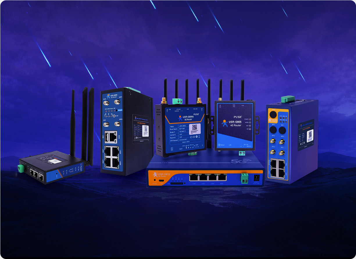
Supported by PUSR's precision welding process, the USR-G806w IoT router has become an ideal choice for high-reliability requirements:
Industrial-Grade Design: It features a metal sheet metal housing (IP30 protection rating), supports a wide operating temperature range of -20°C to 70°C and a humidity resistance of 5% to 95% RH (non-condensing), adapting to complex industrial scenarios such as warehousing, manufacturing, and energy.
Multimodal Communication: It integrates 4G LTE, Wi-Fi, and Ethernet ports (2 LAN and 1 WAN/LAN), supporting intelligent multi-network switching and backup functions for wired/4G/Wi-Fi to ensure continuous data transmission. For example, in an AGV scheduling project on an automobile assembly line, the USR-G806w achieved a data transmission success rate of 99.97% with a network switching delay of less than 30 ms.
Edge Computing Capability: It is equipped with a quad-core ARM Cortex-A7 processor, supporting the deployment of lightweight AI models. It can process 8 channels of 1080P video streams in real-time and identify shelf numbers and obstacle types through the YOLOv5 algorithm, reducing the AGV path replanning time to 80 ms.
Security Protection System: It incorporates functions such as firewalls, NAT, DMZ, and port forwarding, supporting multiple VPN protocols such as IPSec, PPTP, and L2TP to ensure the security of data transmission. For example, in a smart grid project, the USR-G806w achieved real-time communication between substations and control centers through VPN encryption, avoiding the risk of data leakage.
In the "reliability race" of the Industrial Internet of Things, precision welding processes have become a key variable determining success or failure. By establishing a full-process control system encompassing "material control - process design - process control - inspection verification," PUSR controls the cold solder joint rate to below 0.01%, offering industrial customers highly reliable communication solutions. For customers pursuing "zero-interruption" communication, choosing PUSR IoT routers is not just choosing a product but also choosing a complete quality control philosophy.