Optical Component Surface Roughness Out of Spec? How Edge AI Quality Inspection Tears Off the "Invisibility Cloak" of 0.01μm-Level Defects
"This batch of lenses—Ra spec is 0.8nm, but measurements came back at 0.9nm for one batch and 1.2nm for another. The client rejected the whole lot. 870,000 RMB, gone. The QC inspector said they look fine to the naked eye, but the data doesn't lie."
This was posted last month by the quality director of an optical components factory in an industry group chat.
Nobody replied. Because everyone knows—this isn't the first time.
The surface roughness of optical components is the most "silent" killer in the entire optical supply chain. It's not as obvious as cracks. It's not as visible as bubbles. It hides in the peaks and valleys at the nanometer scale, in the undulations of 0.01μm—invisible to the naked eye, untouchable by hand, immeasurable by traditional calipers.
But it's enough to turn an entire batch of precision lenses into scrap.
According to ISO 10110-8, optical surface polish grades range from P1 to P4. P4 grade requires the number of micro-defects per 10mm scan line to be N<3. And the RMS roughness of modern ultra-smooth optical surfaces must typically be controlled between 0.8–1.5nm—what does that mean? A human hair is about 70μm in diameter, or 70,000nm. You need to find a bump of less than 2nm on the cross-section of that hair, and then judge whether it's acceptable.
This isn't quality inspection. This is finding one specific grain of sand in the ocean.
And the vast majority of optical component factories are still doing exactly that—looking for a needle in a haystack.
According to industry practice, an optical component under 50mm in diameter typically has only 3–4 areas measured for surface roughness. Components between 150–400mm get 6–7 areas.
Sounds rigorous? But here's the problem—optical component surface quality is never uniform. The roughness at the center and the edge can differ by an entire grade. You measured the center but not the edge. You measured the top half but missed the bottom half.
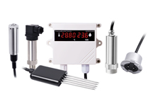
An optical research institute conducted systematic testing using a ZYGO Maxim 3D 5700 surface roughness meter: regarding sampling locations and sample count, generally 6 sampling areas per surface are needed to reflect the overall roughness condition. Too many samples waste time. Too few—you're not measuring product quality, you're measuring luck.
A machine that can measure 0.8nm-level roughness costs several million RMB. One that can measure 0.1nm-level costs over ten million. Equip every production line with one? The cost is unbearable. Can't afford it? Then you do sampling inspection.
What's the consequence of sampling? Data from an auto parts company speaks for itself: equipment downtime caused by sudden tool failure accounts for 22% of total downtime, with an average repair time of 4.2 hours per incident. The same logic applies to optical components—you sampled 10%, missing 90% of the risk. If just one non-conforming piece from that 90% reaches the customer, it's a disaster.
Some factories have installed automated inspection equipment. Data is uploaded to the cloud in real time, algorithms run in the cloud, results come back from the cloud.
Sounds smart. But have you calculated the latency?
In industrial QC scenarios, the latency of traditional backend processing is on the order of "hundreds of milliseconds." An edge computing solution can compress that number to under 20 milliseconds. On a high-speed production line, hundreds of milliseconds means dozens of products have already passed the inspection station. By the time the cloud tells you "unit #37 is non-conforming," units #38, #39, and #40 have already been packaged and shipped.
The cloud is smart. But it's too far from your production line.
In 2026, edge AI has moved past the "proof of concept" stage and officially entered "mass commercial deployment." IDC predicts: by 2030, 50% of enterprise AI inference tasks will migrate from the cloud to edge nodes for local processing.
This isn't a trend. This is happening right now.
The core logic of edge AI QC is fundamentally different from traditional approaches:
| Dimension | Traditional Cloud QC | Edge AI QC |
|---|---|---|
| Data Processing Location | Cloud GPU servers | Industrial gateway next to the production line |
| Inspection Latency | Hundreds of ms ~ seconds | Under 20 ms |
| Data Transfer Volume | All raw data uploaded | Only results + anomaly screenshots uploaded |
| Offline Capability | Network drop = paralysis | Offline buffering, local storage |
| Defect Detection Rate | 85%–90% | 95%+ |
Why can the edge side achieve a higher detection rate? Because the data is analyzed the moment it's generated.
Traditional approach: capture image → upload → cloud analysis → return result. Any jitter, packet loss, or delay anywhere on this chain leads to missed defects.
Edge approach: capture image → local AI model inference → result in under 20 ms → non-conforming units automatically rejected. Data never leaves the factory. Decisions are never delayed.
Measured data from an industrial AI QC solution has already proven this: using edge computing to perform real-time analysis on 5G-transmitted data, it can extract features that are very difficult to capture—such as tiny surface blemishes on products. Industrial defect detection latency dropped from hundreds of milliseconds to under 20 ms, and the product defect miss rate dropped from 3.2% to 0.5%.
The algorithm didn't change. The algorithm just got closer to the data.
You might ask: does an industrial gateway have enough compute power to run an AI QC model?
Yes. And more than you think.
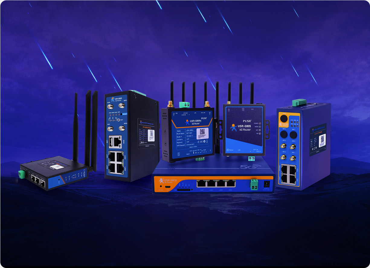
Take PUSR's USR-M300 industrial gateway as an example. This device runs a Linux kernel with a dual-core CPU clocked at up to 1.2 GHz, supporting parallel collection of up to 2,000 data points. It has a built-in Node-RED graphical programming environment—no coding needed, just drag and drop modules to build your own QC logic. It supports Python secondary development, so you can deploy lightweight AI inference models directly on the industrial gateway.
More critically: it supports protocol conversion. Modbus RTU/TCP, OPC UA, Siemens, Mitsubishi, Omron, Inovance—it can adapt and collect from hundreds of common PLC protocols on the market. What does that mean? That old roughness tester on your line, that imported interferometer, that domestic profilometer—no matter what "language" they speak, the M300 understands them all. It can uniformly collect all the data and run AI analysis locally.
It also has a capability traditional solutions can't match: offline buffering. With 2 GB of built-in storage, when the network drops, data is saved locally and automatically retransmitted when the network recovers. Your QC records won't "lose their memory" because of a single network outage.
A real-world case from a photovoltaic company: after introducing edge AI QC, detection response time dropped from 500 ms to 18 ms, and the defect detection rate improved from 91% to 98.7%. The value of silicon wafers saved from scrap in one year exceeded 2 million RMB.
| Metric | Traditional Sampling QC | Edge AI Full Inspection |
|---|---|---|
| Inspection Coverage | 5%–10% | 100% |
| Per-Unit Inspection Time | 30 sec ~ 2 min | <100 ms |
| Defect Detection Rate | 85%–90% | 95%+ |
| Annual Loss from Missed Defects | 500K–2M RMB | <50K RMB |
| Equipment Investment | Single inspection unit 500K+ RMB | Industrial gateway + camera, total <150K RMB |
| Cloud Data Transfer Volume | All raw data | Only anomaly results, reduced by 90%+ |
You see, this isn't about "spending more money on better equipment." It's about spending less money, doing more work, and making fewer mistakes.
The surface roughness of optical components is the most easily overlooked—but most expensive—quality metric in the entire optical supply chain.
Your client won't tell you "surface roughness is out of spec." He'll just tell you "I don't want this batch of lenses." And then you go investigate, and you investigate, and you find out it's because an Ra value of 0.8nm exceeded the spec by 0.1nm.
0.1nm. The diameter of a single atom.
Traditional QC can't catch it. Cloud QC is too slow to catch it. Only edge AI—at the moment the data is generated, at the scale of 0.01μm—can pull it out.
It's 2026. Edge AI QC isn't some black magic. It's the basic survival skill for optical component factories.
PUSR's USR-M300 is built for exactly this. 1.2 GHz dual-core, 2,000-point parallel collection, Node-RED drag-and-drop programming, hundreds of industrial protocols, offline buffering, handles -25°C to 75°C. An engineer deployed edge AI QC across an entire production line in two weeks, saving over 230,000 RMB in equipment procurement costs.
I'm not saying it's the only choice. But if you're being tormented by that 0.01μm defect—it deserves a spot in your top three.
Your optical components don't need a more expensive inspection instrument. They need a brain that's closer. And that brain should be right next to the production line.